Chips

Nvidia's bottleneck

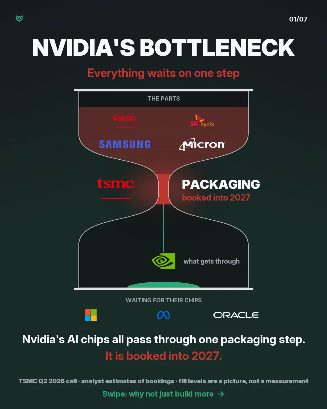
Every AI chip in the world has to pass through one step at one company. It is booked out into 2027.

Numbers as of 21 Aug 2026

The full story

  1. An hourglass. The top bulb is full and holds the parts: TSMC's processor and memory from SK hynix, Samsung and Micron. The neck is plugged solid red and marked packaging, at TSMC, booked into 2027. The bottom bulb is nearly empty: a thin green trickle falls to a small pile with the Nvidia logo on it
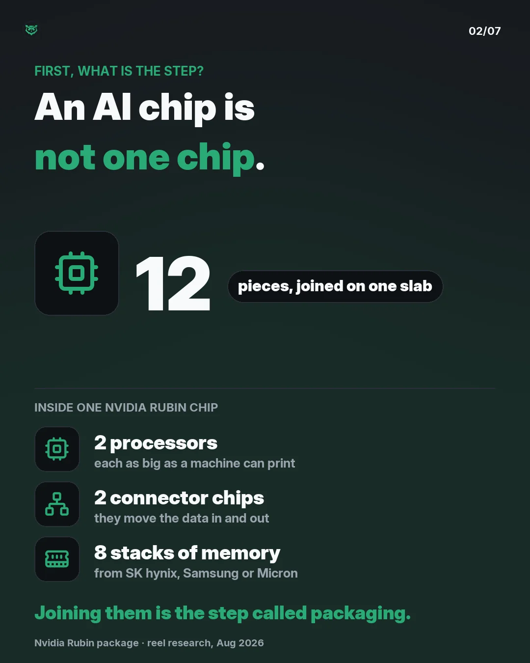
  2. First, what is the step? An AI chip is not one chip. One Nvidia Rubin chip is 12 pieces joined on one slab: 2 processors, each as big as a machine can print, 2 connector chips that move data in and out, and 8 stacks of memory from SK hynix, Samsung or Micron. Joining them is the step called packagin
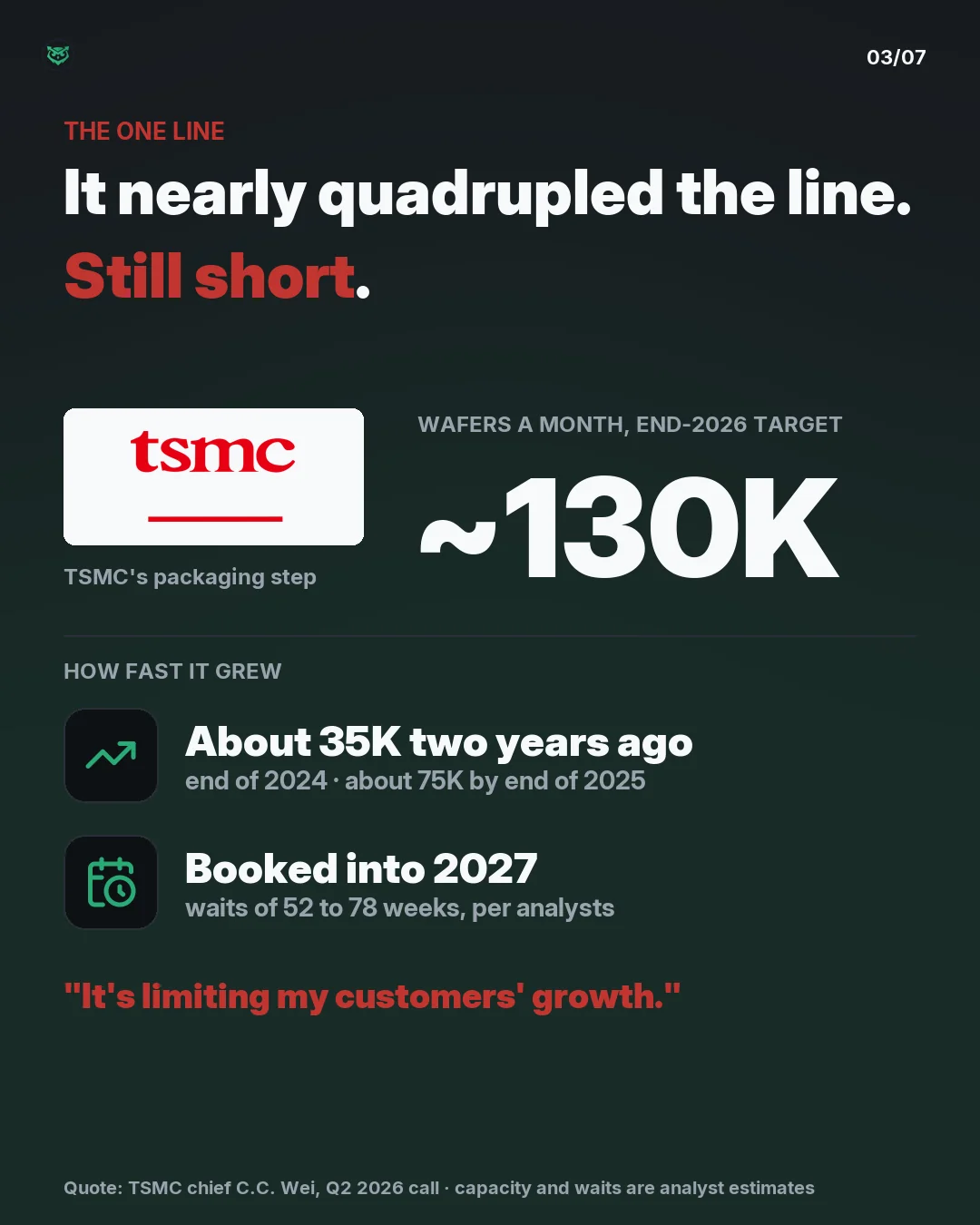
  3. The one line: TSMC's packaging step is targeted at about 130 thousand wafers a month by the end of 2026, nearly four times the 35 thousand of the end of 2024, with about 75 thousand at the end of 2025. It is still short: booked into 2027, with waits of 52 to 78 weeks by analyst estimates. TSMC's chi
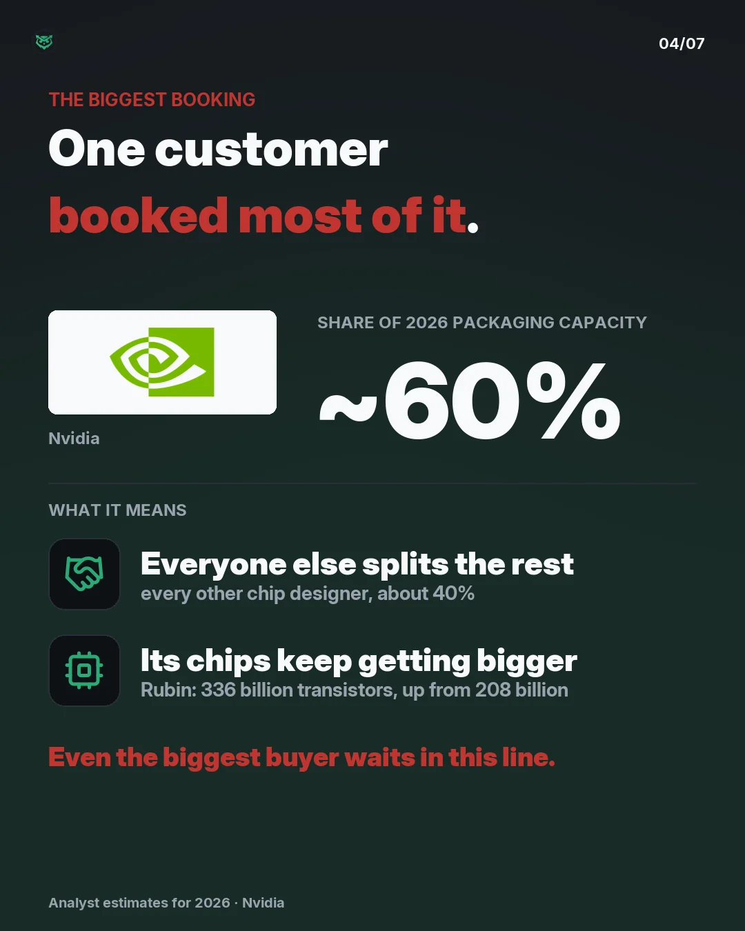
  4. The biggest booking: Nvidia has booked about 60 percent of 2026 packaging capacity, by analyst estimates. Every other chip designer splits about 40 percent. Its chips keep getting bigger: Rubin has 336 billion transistors, up from 208 billion in the chip before. Even the biggest buyer waits in this
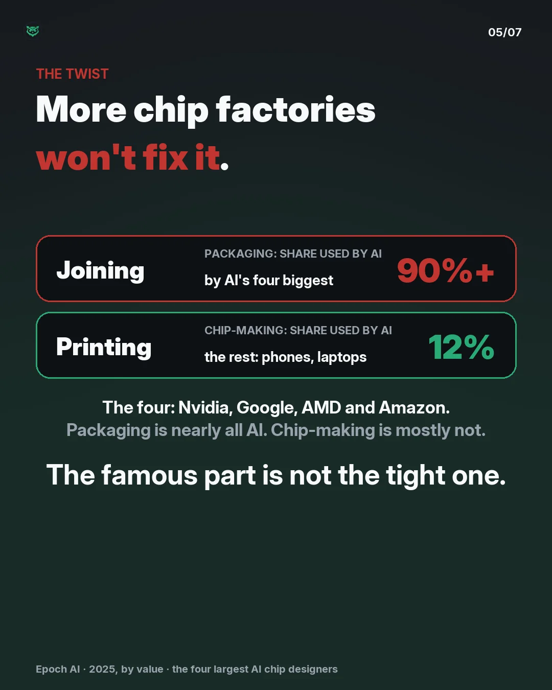
  5. The twist: more chip factories won't fix it. In 2025 the four largest AI chip designers, Nvidia, Google, AMD and Amazon, used more than 90 percent of the world's advanced packaging, the joining step, but only about 12 percent of advanced chip-making; phones, laptops and cars use the rest. The famous
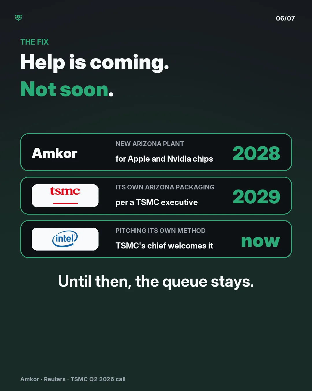
  6. The fix: help is coming, not soon. Amkor's new Arizona plant, for Apple and Nvidia chips, starts production in 2028. TSMC plans its own Arizona packaging by 2029, per a TSMC executive in April 2026. Intel is pitching its own way of joining chips, and TSMC's chief said he welcomes it. Until then, the
  7. Who breaks the bottleneck first? Choices: TSMC, Intel, Samsung, or other. More of the same line, or a rival's? Follow Green Owl if you want more.

An AI chip is not one chip. Nvidia's Rubin package carries two compute dies, two I/O dies and eight memory stacks bonded onto one slab of silicon — and it has to be built that way. Each compute die is already as large as a lithography machine can print in one exposure, so the chip cannot be made bigger, only assembled from more pieces. TSMC calls that step CoWoS.

TSMC said on its Q2 2026 call that packaging is sold out, slots 52 to 78 weeks out, and that the bottleneck is now limiting customer growth.

What the picture simplifies: memory is tight too — all three makers pre-sold their 2026 HBM4 capacity — and a fourth input isn't drawn at all. The ABF substrate the package sits on comes from five firms nobody has heard of, on 20-28 week lead times, and 95% of its core material comes from Ajinomoto. The seasoning company.

Not the constraint: the famous part. Chip designers take ~90% of the world's packaging and memory but only ~12% of advanced logic. More fabs would not fix this.

Estimates. Not financial advice.

Next: what an AI chip costs to build, and who gets paid for each part.
Want to see how this looks now?

When enough people ask, we re-check the numbers and redraw it.

Where the numbers come from

Show all 7 sources

Companies in this picture

More like this